EUV Lithography: The Chain of Physics Behind Advanced Chips
Follow 13.5-nanometre light from tin plasma to a patterned wafer, and learn why optics, vacuum, resist chemistry, and yield matter together.
Reviewed October 11, 2026.
Follow 13.5-nanometre light from tin plasma to a patterned wafer, and learn why optics, vacuum, resist chemistry, and yield matter together.
| Concept | What it means | Important limit |
|---|---|---|
| Light source | 13.5 nm extreme ultraviolet | Source wavelength is not printed feature size |
| Optics | Multilayer reflective mirrors | Ordinary glass lenses absorb EUV |
| Environment | High vacuum | Air would strongly absorb the beam |
| Outcome | Pattern in photoresist | Etch and process control still follow |
1. Lithography transfers geometry rather than carving a whole chip at once
A modern integrated circuit is built through many cycles of depositing material, coating photoresist, exposing a pattern, developing it, etching or implanting, and cleaning. Lithography defines selected geometry for a layer; it does not complete the transistor in one flash. Smaller patterns allow designers to place more elements or improve performance, but dimensions emerge from the entire process. Light wavelength, numerical aperture, mask design, resist behavior, focus, overlay, and computational correction all contribute to what can be manufactured reliably.
2. EUV light begins with droplets of tin
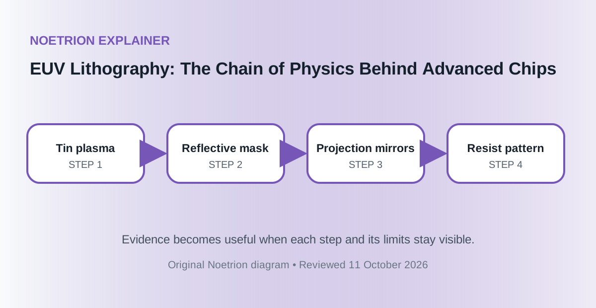
EUV systems use light near 13.5 nanometres. A high-power laser strikes tiny tin droplets, creating a hot plasma that emits a broad range of radiation including the desired EUV band. Collector optics gather part of that emission and direct it into the illumination system. Conversion is difficult: only a fraction of input energy becomes useful in-band light, while debris and heat must be managed. Stable, high average source power matters because wafer throughput depends on delivering repeatable exposure dose many thousands of times.
3. Vacuum and mirrors replace air and glass
Extreme ultraviolet is absorbed strongly by air and by most materials. The optical path therefore operates in vacuum, and conventional transmissive lenses are unusable. Instead, specialized multilayer mirrors reflect a limited fraction of 13.5 nm light through constructive interference. Because every reflection loses energy, mirror quality, contamination control, and the number of optical surfaces matter. The system is less like a camera with glass lenses and more like a precisely aligned sequence of reflective surfaces operating inside an exceptionally clean vacuum environment.
4. The mask is reflective and imperfections matter
The reticle carries the circuit pattern but, like the projection system, must work by reflection. Multilayer structure beneath the absorber pattern can contain defects that influence printed features. A protective pellicle can reduce particle contamination, yet it must transmit EUV while surviving heat. Mask inspection and correction are therefore central engineering tasks. A design that looks geometrically correct in a layout file may require optical proximity correction so that the pattern formed in resist, after diffraction and process effects, matches the designer’s intended shapes.
5. Numerical aperture changes resolution and field geometry
A simplified resolution relationship connects printable pitch with wavelength divided by numerical aperture, multiplied by a process factor. Shorter wavelength and higher numerical aperture can resolve finer structure, but the formula is not a guarantee of yield. Standard EUV tools use 0.33 NA; newer High-NA systems use 0.55 NA and target still smaller features. Higher NA changes depth of focus, optics, masks, exposure field, resist demands, and fab integration. The gain therefore arrives with a redesigned ecosystem rather than a single upgraded lens.
6. Photoresist must be sensitive, sharp, and quiet at once
Photoresist absorbs photons and undergoes chemical changes that allow exposed or unexposed regions to be removed during development. Engineers want high sensitivity for throughput, high resolution for small features, and low roughness for consistent edges. These goals can conflict. At tiny dimensions, the discrete number of photons and chemical events creates stochastic variation: occasional missing contacts, bridges, or rough edges. More exposure dose can reduce some variability but slows throughput. Materials science and process optimization are as important as the nominal wavelength.
7. Overlay connects one layer to every earlier layer
A transistor and its interconnects require many patterned layers aligned within nanometre-scale tolerances. A perfect single-layer image can still fail if it is misplaced relative to earlier structures. The scanner measures wafer position, controls the moving reticle and stage, adjusts focus, and compensates for distortions. Process engineers monitor overlay, critical dimension, defect density, and across-wafer uniformity. EUV is thus a metrology and control problem as much as an illumination problem.
8. Economics is measured in good wafers, not impressive exposure images
Manufacturers care about throughput, availability, consumables, maintenance, process steps, and ultimately functional dies per wafer. EUV can replace several patterning steps that would otherwise be needed with longer-wavelength immersion lithography, simplifying some flows. Yet each EUV layer is expensive, and an additional defect can destroy a valuable die. Decisions about which layers use EUV depend on design rules, tool capacity, yield learning, and total cost. Technical leadership comes from keeping the entire chain stable at production volume.
Conclusion
EUV lithography works because thousands of interacting details—from tin-droplet timing to resist chemistry and stage control—are engineered as one system. The famous 13.5 nm wavelength is only the beginning. Advanced chips appear when that fragile light can repeatedly produce aligned, low-defect patterns fast enough for a factory.